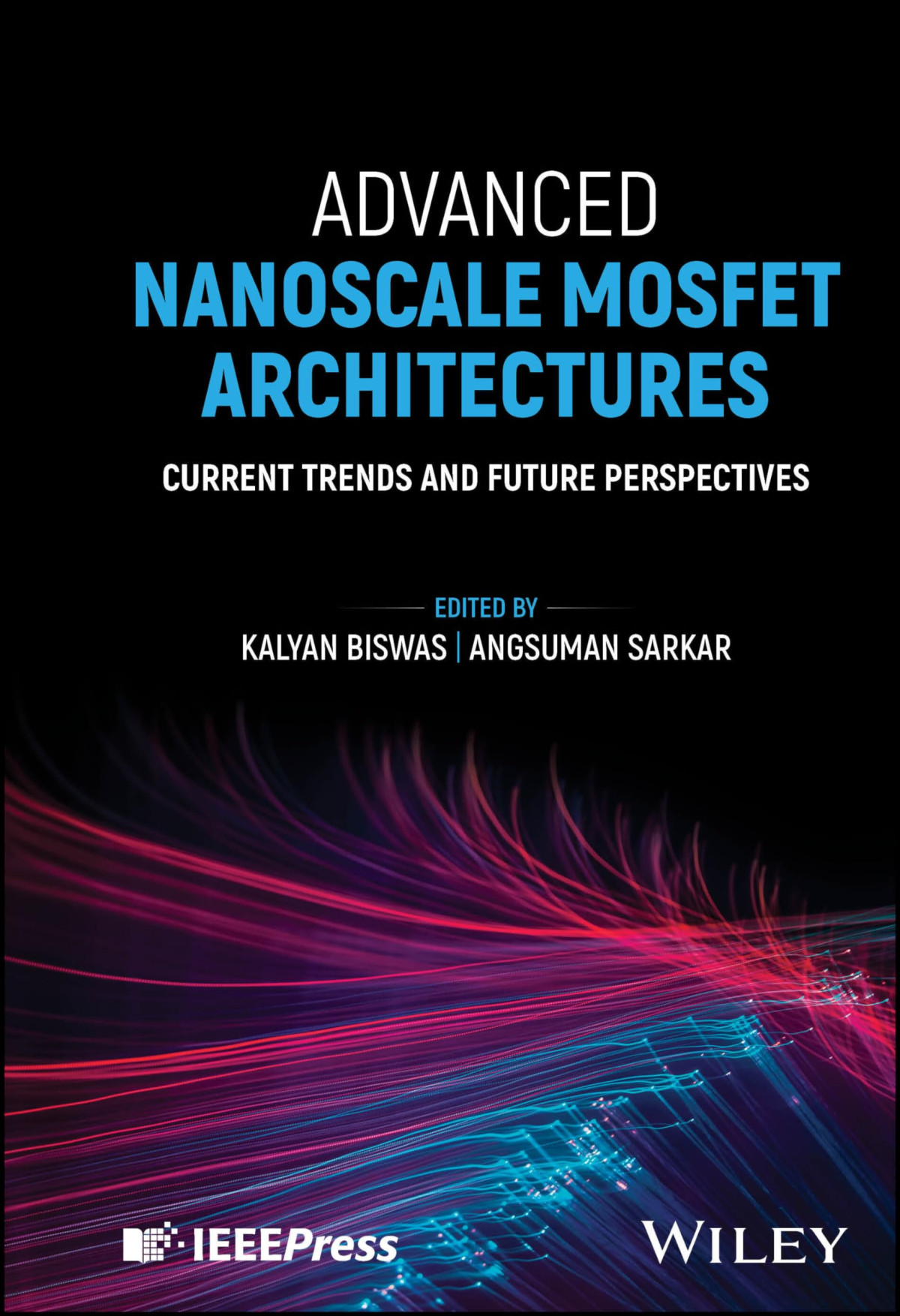
Advanced Nanoscale MOSFET Architectures Current Trends and Future Perspectives 1st Edition by Kalyan Biswas, Angsuman Sarkar 1394188943 9781394188949
$50.00 Original price was: $50.00.$35.00Current price is: $35.00.
Advanced Nanoscale MOSFET Architectures Current Trends and Future Perspectives 1st Edition by Kalyan Biswas, Angsuman Sarkar – Ebook PDF Instant Download/Delivery: 1394188943, 9781394188949
Full download Advanced Nanoscale MOSFET Architectures Current Trends and Future Perspectives 1st Edition after payment

Product details:
ISBN 10: 1394188943
ISBN 13: 9781394188949
Author: Kalyan Biswas, Angsuman Sarkar
Advanced Nanoscale MOSFET Architectures provides an in-depth review of modern metal–oxide–semiconductor field-effect transistor (MOSFET) device technologies and advancements, with information on their operation, various architectures, fabrication, materials, modeling and simulation methods, circuit applications, and other aspects related to nanoscale MOSFET technology.
The text begins with an introduction to the foundational technology before moving on to describe challenges associated with the scaling of nanoscale devices. Other topics covered include device physics and operation, strain engineering for highly scaled MOSFETs, tunnel FET, graphene based field effect transistors, and more. The text also compares silicon bulk and devices, nanosheet transistors and introduces low-power circuit design using advanced MOSFETs.
Additional topics covered include:
- High-k gate dielectrics and metal gate electrodes for multi-gate MOSFETs, covering gate stack processing and metal gate modification
- Strain engineering in 3D complementary metal-oxide semiconductors (CMOS) and its scaling impact, and strain engineering in silicon–germanium (SiGe) FinFET and its challenges and future perspectives
- TCAD simulation of multi-gate MOSFET, covering model calibration and device performance for analog and RF applications
- Description of the design of an analog amplifier circuit using digital CMOS technology of SCL for ultra-low power VLSI applications
Advanced Nanoscale MOSFET Architectures helps readers understand device physics and design of new structures and material compositions, making it an important resource for the researchers and professionals who are carrying out research in the field, along with students in related programs of study.
Table of contents:
1 Emerging MOSFET Technologies
1.1 Introduction: Transistor Action
1.2 MOSFET Scaling
1.3 Challenges in Scaling the MOSFET
1.4 Emerging MOSFET Architectures
1.5 Organization of this Book
References
2 MOSFET: Device Physics and Operation
2.1 Introduction to MOSFET
2.2 Advantages of MOSFET
2.3 Applications of MOSFETs
2.4 Types of MOSFETs
2.5 Band Diagram of MOSFET
2.6 MOSFET Regions of Operation
2.7 Scaling of MOSFET
2.8 Short‐channel Effects
2.9 Body Bias Effect
2.10 Advancement of MOSFET Structures
References
3 High‐κ Dielectrics in Next Generation VLSI/Mixed Signal Circuits
3.1 Introduction to Gate Dielectrics
3.2 High‐κ Dielectrics in Metal–Oxide–Semiconductor Capacitors
3.3 High‐κ Dielectrics in Metal Insulator Metal (MIM) Capacitors
3.4 MOSFETs Scaling and the Need of High‐κ
3.5 High‐κ Dielectrics in Next Generation Transistors
References
4 Consequential Effects of Trap Charges on Dielectric Defects for MU‐G FET
4.1 Introduction
4.2 TID Effects Overview
4.3 Application Area of Device for TID Effect Analysis
4.4 Near the Earth: Trapped Radiation
4.5 Ionizing Radiation Effect in Silicon Dioxide (SiO2)
4.6 TID Effects in CMOS
4.7 TID Effects in Bipolar Devices
4.8 Understanding and Modeling a‐SiO2 Physics
4.9 Hydrogen (H2) Reaction with Trapped Charges at Insulator
4.10 Pre‐Existing Trap Density and their Respective Location
4.11 Use of High‐K Dielectric in MU‐G FET
4.12 Properties of Trap in the High‐K with Interfacial Layer
4.13 Trap Extraction Techniques
4.14 Conclusion
References
5 Strain Engineering for Highly Scaled MOSFETs
5.1 Introduction
5.2 Simulation Approach
5.3 Case Study
5.4 Conclusions
References
6 TCAD Analysis of Linearity Performance on Modified Ferroelectric Layer in FET Device with Spacer
6.1 Introduction
6.2 Simulation and Structure of Device
6.3 Results and Analysis
6.4 Conclusion
Acknowledgment
References
7 Electrically Doped Nano Devices: A First Principle Paradigm
7.1 Introduction
7.2 Electrical Doping
7.3 First Principle
7.4 Molecular Simulation
7.5 Conclusion
References
8 Tunnel FET: Principles and Operations
8.1 Introduction to Quantum Mechanics and Principles of Tunneling
8.2 Tunnel Field‐Effect Transistor
8.3 Challenges of Tunnel Field‐Effect Transistor
8.4 Techniques for Improving Electrical Performance of Tunnel Field‐Effect Transistor
8.5 Conclusion
References
9 GaN Devices for Optoelectronics Applications
9.1 Introduction
9.2 Properties of GaN‐Based Material
9.3 GaN LEDs
9.4 GaN Lasers
9.5 GaN HEMTs for Optoelectronics
9.6 GaN Sensors
References
10 First Principles Theoretical Design on Graphene‐Based Field‐Effect Transistors
10.1 Introduction
10.2 Graphene
10.3 Graphene/ ‐BN Hybrid Structure
10.4 Conclusions
Acknowledgments
References
11 Performance Analysis of Nanosheet Transistors for Analog ICs
11.1 Introduction
11.2 Evolution of Nanosheet Transistors
11.3 TCAD Modeling of Nanosheet Transistor
11.4 Transistor’s Analog Performance Parameters
11.5 Challenges and Perspectives of Modern Analog Design
References
12 Low‐Power Analog Amplifier Design using MOS Transistor in the Weak Inversion Mode
12.1 Introduction
12.2 Review of the Theory of Weak Inversion Mode Operation of MOS Transistor
12.3 Design Steps for Transistor Sizing Using the IC
12.4 Design Examples
12.5 Summary
References
13 Ultra‐conductive Junctionless Tunnel Field‐effect Transistor‐based Biosensor with Negative Capacitance
13.1 Introduction
13.2 Importance of SS and I ON/I OFF in Biosensing
13.3 Importance of Dopingless Source and Drain in High Conductivity
13.4 Relation of Negative Capacitance with Non‐hysteresis and Effect on Biosensing
13.5 Variation of Source Material on Biosensing
13.6 Importance of Dual Gate and Ferroelectricity on Biosensing
13.7 Effect of Dual Material Gate on Biosensing
References
14 Conclusion and Future Perspectives
14.1 Applications
14.2 Some Recent Developments
14.3 Future Perspectives
14.4 Conclusion
People also search:
advanced power mosfet
nanoscale transistors
advanced cmos technology
advanced nodes
nanoscale mosfet modeling
Tags: Kalyan Biswas, Angsuman Sarkar, Advanced, Nanoscale


