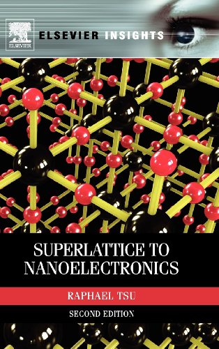
Superlattice to Nanoelectronics 2nd Edition by Raphael Tsu 0080968139 9780080968131
$50.00 Original price was: $50.00.$35.00Current price is: $35.00.
Superlattice to Nanoelectronics 2nd Edition by Raphael Tsu – Ebook PDF Instant Download/Delivery: 0080968139, 9780080968131
Full download Superlattice to Nanoelectronics 2nd Edition after payment

Product details:
ISBN 10: 0080968139
ISBN 13: 9780080968131
Author: Raphael Tsu
Written by one of the founders of this field, this book provides a historical overview of the invention of superlattice, one of the most important devices of the second half of the 20th century. In addition to describing the fundamental concepts, this completely revised and updated edition provides new insights in the field of manmade solids.
- Written by one of the founders of this field
- Delivers over 20% new material, including new research and new technological applications
-
Provides a basic understanding of the physics involved from first principles, while adding new depth, using basic mathematics and an explanation of the background essentials
Table of contents:
Chapter 1 Superlattice
1.1 The Birth of the Man-Made Superlattice
1.2 A Model for the Creation of Man-Made Energy Bands
1.3 Transport Properties of a Superlattice
1.4 More Rigorous Derivation of the NDC
1.5 Response of a Time-Dependent Electric Field and Bloch Oscillation
1.6 NDC from the Hopping Model and Electric Field–Induced Localization
1.7 Experiments
1.8 Type-III Superlattice (Historically Type-II Superlattice)
1.9 Physical Realization and Characterization of a Superlattice
1.10 Summary
Chapter 2 Resonant Tunneling via Man-Made Quantum Well States
2.1 The Birth of Resonant Tunneling
2.2 Some Fundamentals
2.3 Conductance from the Tsu–Esaki Formula
2.4 Tunneling Time from the Time-Dependent Schrödinger Equation
2.5 Damping in Resonant Tunneling
2.6 Very Short l and w for an Amorphous QW
2.7 Self-Consistent Potential Correction of DBRT
2.8 Experimental Confirmation of Resonant Tunneling
2.9 Instability in RTD
2.10 Summary
Chapter 3 Optical Properties and Raman Scattering in Man-Made Quantum Systems
3.1 Optical Absorption in a Superlattice
3.2 Photoconductivity in a Superlattice
3.3 Raman Scattering in a Superlattice and QW
3.4 Summary
Chapter 4 Dielectric Function and Doping of a Superlattice
4.1 Dielectric Function of a Superlattice and a Quantum Well
4.2 Doping a Superlattice
4.3 Summary
Chapter 5 Quantum Step and Activation Energy
5.1 Optical Properties of Quantum Steps
5.2 Determination of Activation Energy in Quantum Wells
5.3 Summary
Chapter 6 Semiconductor Atomic Superlattice (SAS)
6.1 Silicon-Based Quantum Wells
6.2 Si-Interface Adsorbed Gas (IAG) Superlattice
6.3 Amorphous Silicon/Silicon Oxide Superlattice
6.4 Silicon–Oxygen (Si–O) Superlattice
6.5 Estimate of the Band-Edge Alignment Using Atomic States
6.6 Estimate of the Band-Edge Alignment with HOMO–LUMO
6.7 Estimation of Strain from a Ball-and-Stick Model
6.8 Electroluminescence and Photoluminescence
6.9 Transport through a Si–O Superlattice
6.10 A Si–O Superlattice and Other Si/Ge, Si/Co, Si/C Monolayer Superlattice
6.11 Summary
Chapter 7 Si Quantum Dots
7.1 Energy States of Silicon Quantum Dots
7.2 Resonant Tunneling in Silicon Quantum Dots
7.3 Slow Oscillations and Hysteresis
7.4 Avalanche Multiplication from Resonant Tunneling
7.5 Influence of Light and Repeatability under Multiple Scans
7.6 Many Body Effects in Coupled Quantum Dots
7.7 Summary
Chapter 8 Capacitance, Dielectric Constant, and Doping Quantum Dots
8.1 Capacitance of Silicon Quantum Dots
8.2 Dielectric Constant of a Silicon Quantum Dot
8.3 Doping a Silicon Quantum Dot
8.4 Capacitance: Spatial Symmetry of Discrete Charge Dielectric
8.5 Summary
Chapter 9 Porous Silicon
9.1 Porous Silicon: Light-Emitting Silicon
9.2 PSi: Other Applications
9.3 Summary
Chapter 10 Some Novel Devices
10.1 Field Emission with Quantum Well and Nanometer Thick Multilayer Structured Cathode
10.2 Saturation Intensity of PbS QDs
10.3 Multipole Electrode Heterojunction Hybrid Structures
10.4 Some Fundamental Issues: Mainly Difficulties
10.5 Comments on Quantum Computing
10.6 Recent Activities in Superlattice
10.7 Graphene Adventure
10.8 Summary
Chapter 11 Quantum Impedance of Electrons
11.1 Landauer Conductance Formula
11.2 Electron Quantum Waveguide
11.3 Wave Impedance of Electrons
11.4 Summary
Chapter 12 Why Super and Why Nano?
12.1 Finite Solid, Giant Molecule, and Composite
12.2 Generalization of Superlattices into Components
12.3 QDs as Individual Components
12.4 Size Requirements
12.5 Superlattice and the World of Nano
12.6 Some New Opportunities
12.7 A Word of Caution
People also search:
superlattice to nanoelectronics
nanoparticle superlattice
superlattice nanowire pattern transfer
c convert nanoseconds to seconds
nano superlattice
Tags: Raphael Tsu, Superlattice, Nanoelectronics


