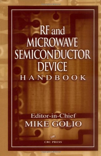
RF and Microwave Semiconductor Device Handbook 1st Edition by Mike Golio 1498798047 9781498798044
$50.00 Original price was: $50.00.$35.00Current price is: $35.00.
RF and Microwave Semiconductor Device Handbook 1st Edition by Mike Golio – Ebook PDF Instant Download/Delivery: 1498798047, 9781498798044
Full download RF and Microwave Semiconductor Device Handbook 1st Edition after payment

Product details:
ISBN 10: 1498798047
ISBN 13: 9781498798044
Author: Mike Golio
Offering a single volume reference for high frequency semiconductor devices, this handbook covers basic material characteristics, system level concerns and constraints, simulation and modeling of devices, and packaging. Individual chapters detail the properties and characteristics of each semiconductor device type, including: Varactors, Schottky diodes, transit-time devices, BJTs, HBTs, MOSFETs, MESFETs, and HEMTs. Written by leading researchers in the field, the RF and Microwave Semiconductor Device Handbook provides an excellent starting point for programs involving development, technology comparison, or acquisition of RF and wireless semiconductor devices.
RF and Microwave Semiconductor Device Handbook 1st Table of contents:
1 Varactors
1.1 Introduction
1.2 Basic Concepts
1.3 Varactor Applications
1.4 Varactor Devices
2 Schottky Diode Frequency Multipliers
2.1 Introduction
2.2 Schottky Diode Characteristics
2.3 Analytic Descriptions of Diode Multipliers
2.4 Computer-Based Design Approaches
2.5 Device Limitations and Alternative Device Structures
2.6 Summary and Conclusions
3 Transit Time Microwave Devices
3.1 Introduction
3.2 Semiconductor Material Properties
3.3 Two-Terminal Active Microwave Devices
Defining Terms
4 Bipolar Junction Transistors
4.1 Introduction
4.2 Basic Operation
5 Heterostructure Bipolar Transistors
5.1 Basic Device Principle
5.2 Base Current Components
5.3 Kirk Effects
5.4 Collapse of Current Gain
5.5 High Frequency Performance
5.6 Device Fabrication
6 Metal-Oxide-Semiconductor Field-Effect Transistors
6.1 Introduction
6.2 MOSFET Fundamentals
6.3 CMOS at Radio Frequencies
6.4 MOSFET Noise Sources
6.5 MOSFET Design for RF Operation
6.6 MOSFET Layout
6.7 The Future of CMOS
7 Metal Semiconductor Field Effect Transistors
7.1 Introduction
7.2 Principle of Operation
7.3 Properties of Semiconductor Materials Used in MESFET Technology
7.4 Schottky Barrier Contacts
7.5 MESFET Technology
7.6 MESFET Modeling
7.7 Hetero-Dimensional (2D MESFETs)
7.8 Applications
8 High Electron Mobility Transistors
8.1 Introduction
8.2 HEMT Device Operation and Design
8.3 Scaling Issues in Ultra-High-Speed HEMTs
8.4 Material Systems for HEMT Devices
8.5 AlGaAs/InGaAs/GaAs Pseudomorphic HEMT (GaAs pHEMT)
8.6 AlInAs/GaInAs/InP (InP HEMT)
8.7 Technology Comparisons
8.8 Conclusion
9 RF Power Transistors from Wide Bandgap Materials
9.1 Introduction
9.2 Figures of Merit for RF Power Transistors
9.3 Common RF Power Devices from Wide Bandgap Materials
9.4 Desirable Material Properties for RF Power Transistors
9.5 State-of-the-Art Wide Bandgap Microwave Transistor Data
9.6 Challenges to Production
9.7 Conclusion
10 Monolithic Microwave IC Technology
10.1 Overview
10.2 Basic Principles of GaAs MESFETs and HEMTs
10.3 MMIC Lumped Elements: Resistors, Capacitors, and Inductors
10.4 MMIC Processing and Mask Sets
Defining Terms
11 Semiconductors
11.1 Introduction
11.2 Silicon
11.3 Gallium Arsenide
11.4 III-V Heterostructures
11.5 Indium Phosphide
11.6 Silicon Carbide
11.7 Gallium Nitride
11.8 Selected Material Properties
11.9 Etching Processes for Semiconductors
11.10 Ohmic and Schottky Contacts
12 Metals
12.1 Introduction
12.2 Resistance, Resistivity, and Conductivity
12.3 Skin Depth
12.4 Heat Conduction
12.5 Temperature Expansion
12.6 Chemical Properties
12.7 Weight
13 RF Package Design and Development
13.1 Introduction
13.2 Thermal Management
13.3 Mechanical Design
13.4 Package Electrical and Electromagnetic Modeling
13.5 Design Verification, Materials, and Reliability Testing
13.6 Computer-Integrated Manufacturing
13.7 Conclusions
14 Thermal Analysis and Design of Electronic Systems
14.1 Motivation
14.2 Thermal Modeling
14.3 Thermal Resistance Networks
15 Low Voltage/Low Power Microwave Electronics
15.1 Introduction
15.2 Motivations for Reduced Voltage
15.3 Semiconductor Materials Technology
15.4 Semiconductor Device Technology
15.5 Circuit Design
15.6 Radio and System Architecture
15.7 Limits to Reductions in Voltage
15.8 Summary
16 Technology Computer Aided Design
16.1 Introduction
16.2 An Overview of TCAD
16.3 Benefits of TCAD
16.4 Limitations of TCAD
16.5 The Role of Calibration
16.6 Applications of TCAD
16.7 Application Protocols
16.8 Conclusions
17 Nonlinear Transistor Modeling for Circuit Simulation
17.1 Modeling in General
17.2 Scope of This Work
17.3 Equivalent Circuit Models
17.4 SPICE Models and Application-Specific Models
17.5 Improved Transistor Models for Circuit Simulation
17.6 Modeling Gate Charge as a Function of Local and Remote Voltages in MESFETS and PHEMTS
17.7 Modeling the Effects Due to Traps
17.8 Modeling Temperature Effects and Self-Heating
17.9 Enhancing the Gummel-Poon Model for Use with GaAs and InP HBTs
17.10 Modeling the RF LDMOS Power Transistor
17.11 Parameter Extraction for Analytical Models
17.12 The Vector Nonlinear Network Analyzer
17.13 Model Verification
17.14 Foundry Models and Statistics
17.15 Future Nonlinear Transistor Models
People also search for RF and Microwave Semiconductor Device Handbook 1st:
rf and microwave semiconductor device handbook
rf and microwave design
rf and microwave components
rf and microwave engineering fundamentals of wireless communications pdf
Tags:
Mike Golio,Microwave,Semiconductor,Device


